PCBA Visual Inspection and Quality Control
Before a board powers up, it reveals much about its alignment, precision, and the craftsmanship of its automated assembly. Despite modern SMT processes, even the smallest flaw can lead to major failures later.
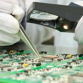
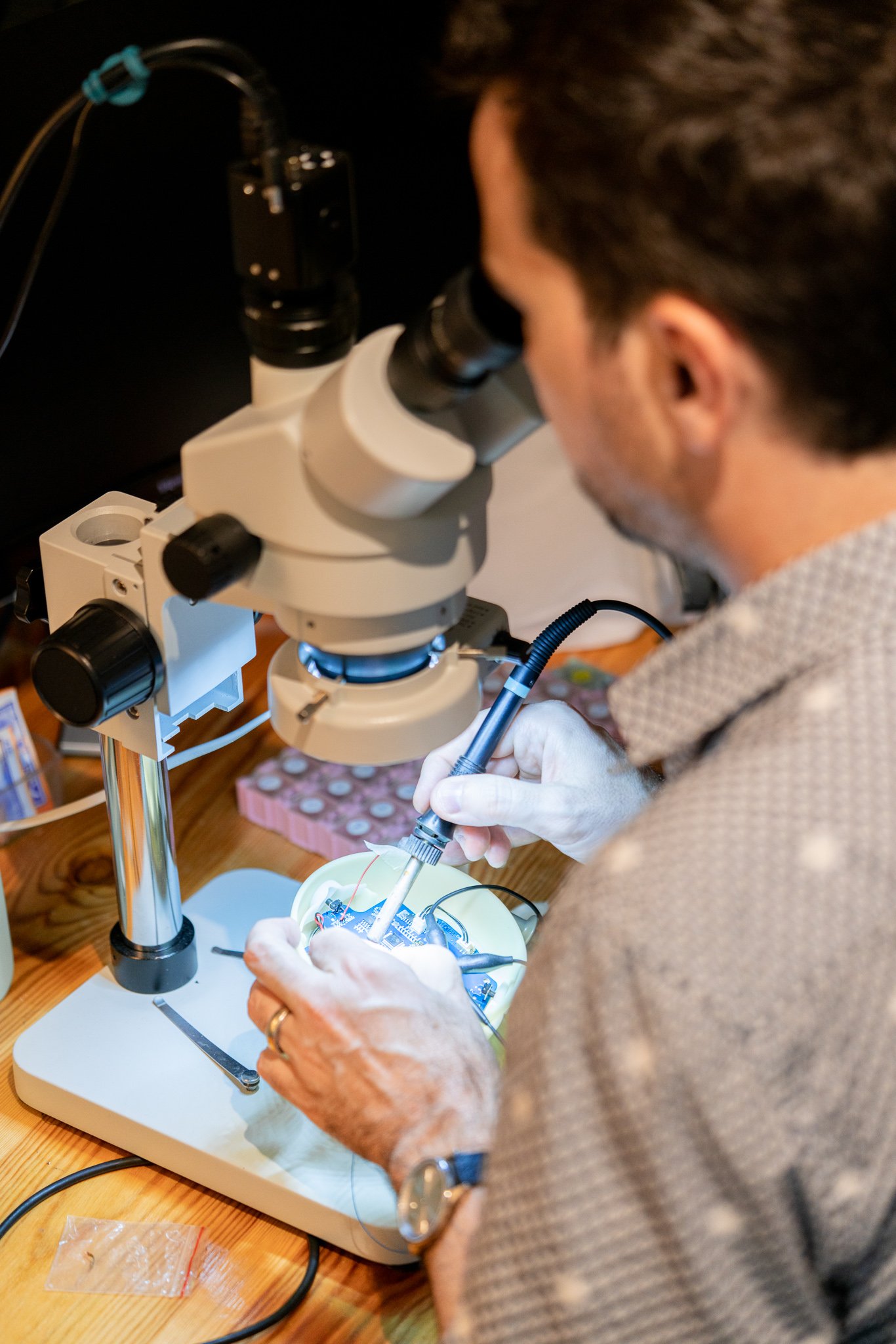
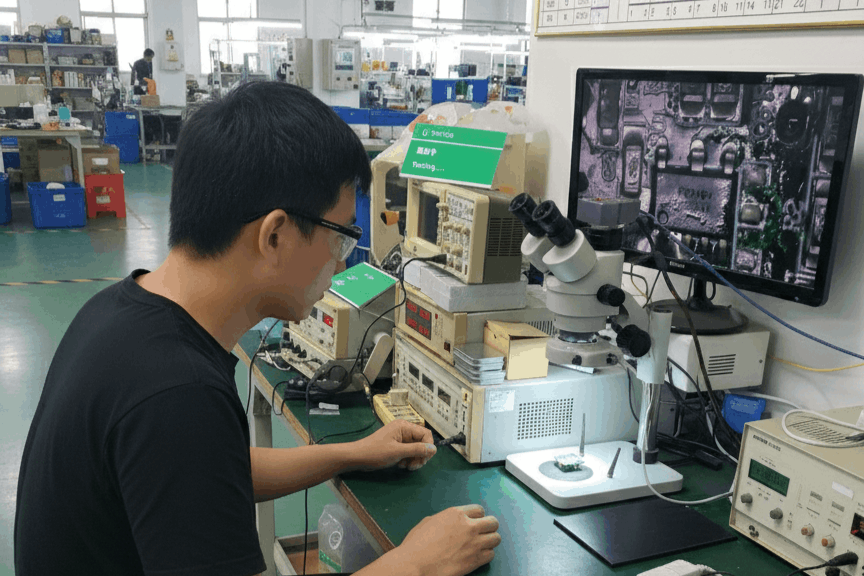
We examine each PCBA using magnification and structured inspection criteria. This includes checking solder joints, part alignment, lead conditions, flux residue, pad wetting, component height, and any signs of cold solder joints or bridging. We compare our findings to IPC standards and our internal data. When we notice a recurring issue—even one that hasn’t caused a failure—we trace it back to the specific process or machine setting responsible.
PCBA Visual inspection is the first opportunity to spot manufacturing drift. Identifying issues early helps avoid intermittent faults, boosts long-term reliability, and reduces time spent fixing problems during firmware development.
What We Do
Each product unit relies on a carefully assembled and calibrated PCB to operate efficiently. Using a microscope, our Tektos Ecosystems quality engineers examine the circuit board during production to catch microscopic issues such as:
Misaligned surface-mount components – even a slight shift can impact functionality.
Cold or cracked solder joints – these can lead to intermittent failures over time.
Solder bridging or open circuits – preventing short circuits and ensuring uninterrupted operation.
Contaminants like dust or flux residue – which can interfere with signal integrity or cause corrosion.
This step is done before any firmware upload or enclosure assembly, ensuring only flawless boards move forward.
Why It Matters
Even a tiny solder flaw can cause sensor drift,
connectivity drops, or complete device failure.
By catching these issues early under the microscope,
we prevent downstream problems and
ensure your product performs with the accuracy,
stability, and reliability it was designed for—right out of the box.
Our meticulous PCBA inspection process is just one example
of how we uphold our quality promise. At Tektos Ecosystems,
invisible issues aren’t acceptable—even if you’d never see them, we do.
By addressing them upfront, we protect the integrity
of your product and the experience of your end users.